Overview
I first got the circuit working on a breadboard, powered by a 9 V battery. Then I turned that design into a real PCB. Going from breadboard to board taught me a lot I hadn't run into before: matching footprints to real parts, choosing component ratings, design rules from the fab house, and keeping a schematic clean enough that someone else could read it.
The circuit
The circuit is a classic two-transistor astable multivibrator. Two 2N3904 NPN transistors are cross-coupled through 10 µF capacitors. When one transistor switches on, its capacitor yanks the other transistor's base negative and holds it off. The base then recharges through its 100 kΩ resistor until that transistor switches on, and the cycle flips. The result is a steady back-and-forth with no microcontroller at all.
Each side drives two common-cathode RGB LEDs. Only the red and blue channels are used, which mixes to pink. With 100 kΩ and 10 µF, each half-cycle lasts roughly 0.7 seconds (t ≈ 0.693 · R · C).
Parts
I sourced every part from Mouser and matched each one to a KiCad footprint using its datasheet: body size, lead pitch, and lead diameter.
| Part | Qty | Mouser part |
|---|---|---|
| 2N3904 NPN transistor | 2 | Diotec Semiconductor 2N3904 (637-2N3904) |
| 10 µF 16 V electrolytic capacitor | 2 | Würth 860010372001 |
| 100 kΩ ½ W metal oxide resistor | 2 | Yageo RSF-50JT-52-100K |
| 220 Ω ½ W metal oxide resistor | 14 | Stackpole RSPF12JT220R |
| 5 mm RGB LED, common cathode | 4 | Soldered 100105 |
| 9 V battery snap (soldered to board) | 1 | Ordered from Amazon |
Schematic
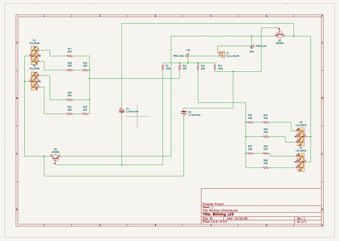
Reviewing the schematic turned up several mistakes that would have caused real problems on the board:
- Wrong LED symbol. I first used a common-anode symbol, but my LEDs are common-cathode, with the shared lead on pin 2. I switched to
LED_RKGB, which matches the physical pin order (red, cathode, green, blue). - Reversed capacitor. C5 was mirrored, with its + terminal on the transistor base. In this circuit the base side swings negative, so + has to face the collector. A backwards electrolytic can still run on the bench while it slowly degrades, so now I check every polarized part.
- Resistors that did nothing. Two 10 Ω resistors were in series with 220 Ω ones. 10 Ω is less than the 220 Ω part's own ±5% tolerance (±11 Ω), so I removed them.
- LEDs sharing a resistor. LEDs in parallel on one resistor share current unevenly, so their brightness and color differ. I gave each LED color its own resistor.
- No way to connect power. On a breadboard, +9 V and GND come from the rails. A PCB needs a real connector, so I added J1 for the battery wires, plus
PWR_FLAGsymbols so the electrical rules check passes.
PCB layout
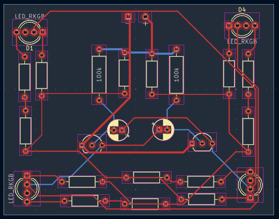
I set up the design rules from JLCPCB's 2-layer capabilities. I learned that design rules come from the fab, while footprints come from the parts. The fab's minimums are the floor for the design rule check (DRC), not the widths to actually route with.
| Rule | Value |
|---|---|
| Min track width / clearance (fab limit) | 0.127 mm |
| Min via drill / diameter | 0.3 mm / 0.5 mm |
| Min annular ring | 0.15 mm |
| Default signal traces | 0.3 mm |
| Power traces (+9 V, GND) | 0.5 mm |
Cleaning up the board
- DRC errors on tight footprints. The TO-92 transistors and RGB LEDs have leads only 1.27 mm apart, which caused 35 clearance and annular-ring errors. I didn't lower the board-wide clearance to hide them, because that would also hide real problems. Final DRC: zero errors and zero unconnected items.
- Trace angles. I rerouted traces to 0°, 45°, and 90° only.
- A stray track ran around the entire board edge. Deleting it cleared the last unconnected item.
- Silkscreen. I removed confusing value labels but kept "100k" on the two 100 kΩ resistors, the parts most likely to get swapped during assembly. I also added real + and − marks at the battery pads, since net names shown in KiCad pads aren't printed on the board.
- Placement. I placed the LEDs so diagonal pairs blink together. That looks better, but it meant longer traces. Next time I'll group each half of the mirrored circuit together.
Fabrication
I exported Gerbers (copper, silkscreen, solder mask, and board outline layers) and Excellon drill files from KiCad. I ordered the boards from JLCPCB: 2 layers, 1.6 mm thick, HASL finish, green solder mask, 1 oz copper. Boards and parts were ordered on October 27, 2026.
Planned assembly order: resistors first, then the transistors and capacitors, then the LEDs last. Before connecting the battery, I'll check with a multimeter that +9 V and GND aren't shorted.